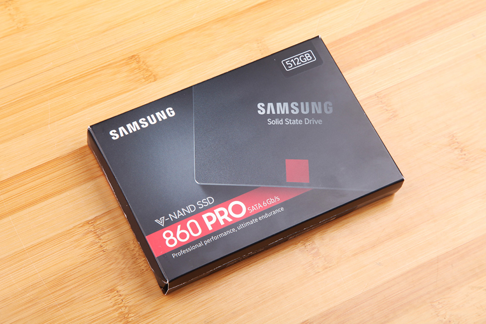
In early 2014, Samsung introduced the first 3D flash, the 850 PRO/EVO, to the consumer market. About four years later, Samsung released the 860 PRO/EVO, an upgraded version of the 850 PRO/EVO. Today, we will start to tear down the Samsung 860 PRO 512GB SSD.
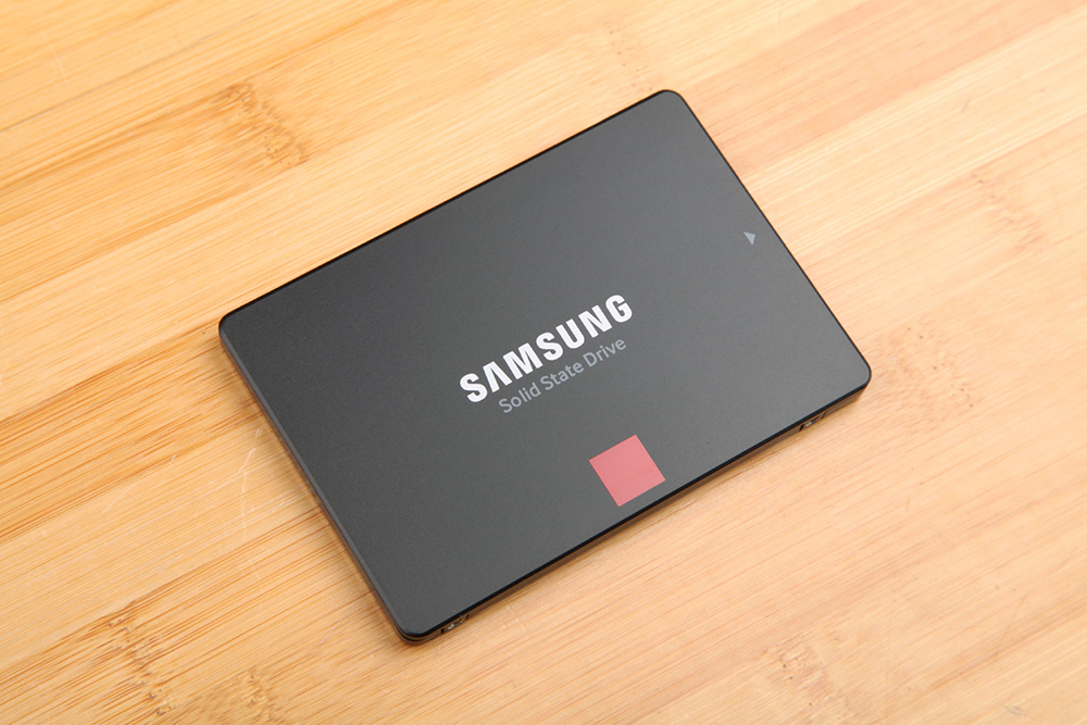
The Samsung 860 PRO is about 2.5 inches large. In the front of the SSD, we can see “Samsung” and “Solid State Drive” without the product model number. The red square is below the words. The arrow mark on the right indicates the port direction.
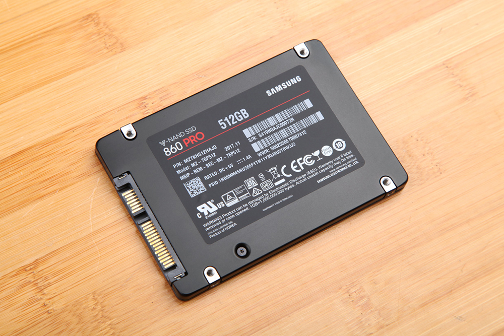
The back of the SSD contains more information, including the model number, capacity, production date, operating voltage, operating current, and so on. The 512GB 860 PRO that we will disassemble was made in November 2017.
The hardware port on the left is the SATA 3.0, and its theoretical wideband is 6Gb/s. The power port is on the right. The SSD’s maximum sequential read speed reaches 560MB/s, and its maximum sequential write speed reaches 530MB/s. The SSD has random read speeds of up to 100K IOPS and random write speeds of up to 90K IOPS. The SSD with the SATA 3.0 interface doesn’t have as fast a speed as a SATA SSD.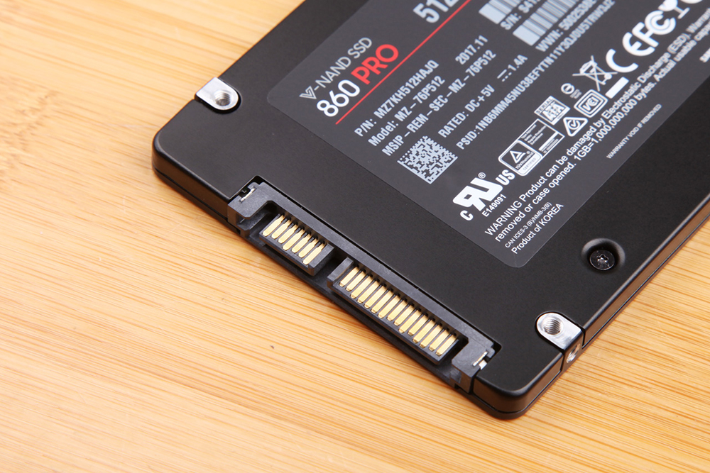
Remove the screws from the back. The SSD uses a pentagon screw, which is not common to see. After removing the back cover, we found that the PCB of the 860 PRO is quite small. The size of the PCB is just the 1/3 of the SSD.
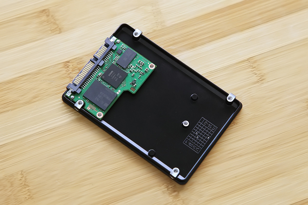
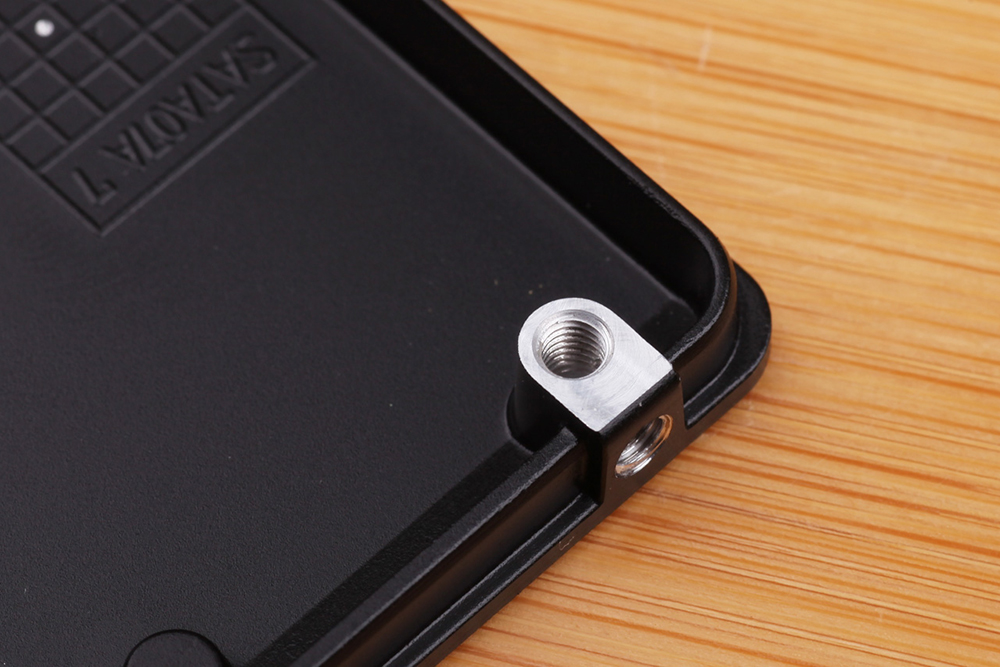
Generally speaking, the screws on the SSD can’t be separated from the back. However, the screw port on the back of the Samsung 860 PRO SSD is connected to the screw port on the side. The surfaces are all polished. The fixed method that the 860 PRO SSD applies to is better than the common fixed method that SSD uses. Of course, this fixed method has a higher demand on the front SSD’s hardness.
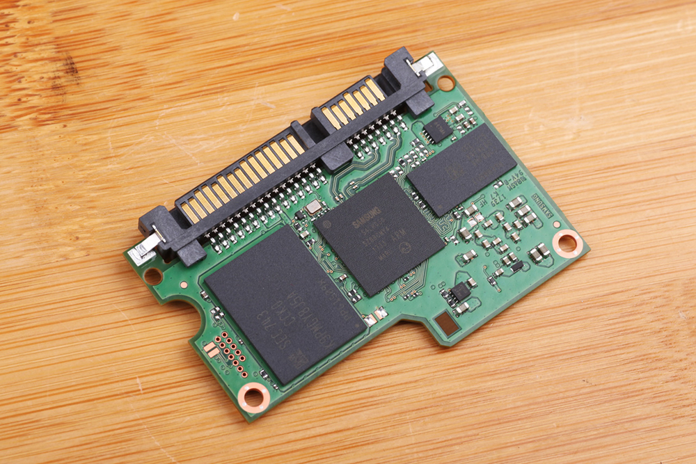
The front PCB is composed of a master control, a cache chip, a flash, and lots of capacitors.
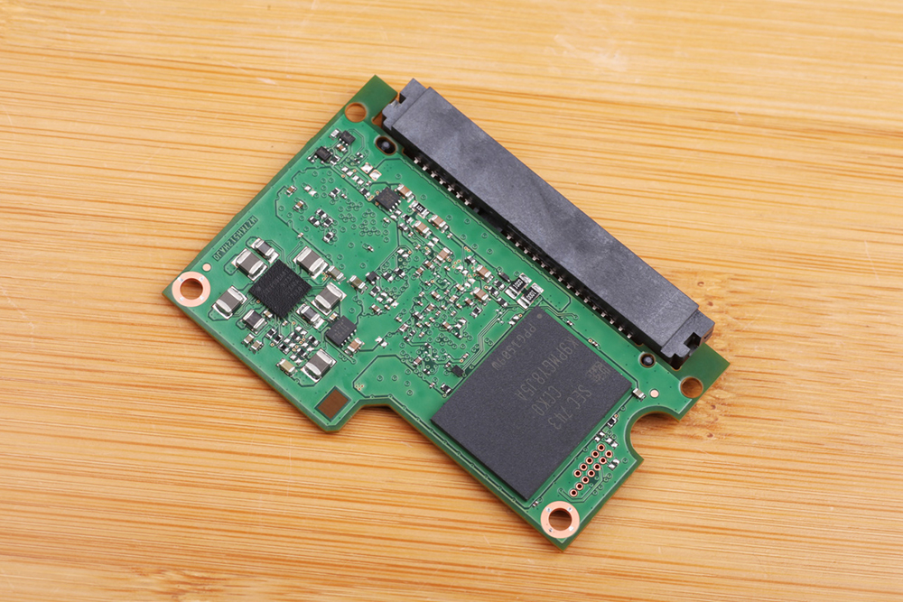
There is only a flash on the back of the PCB.
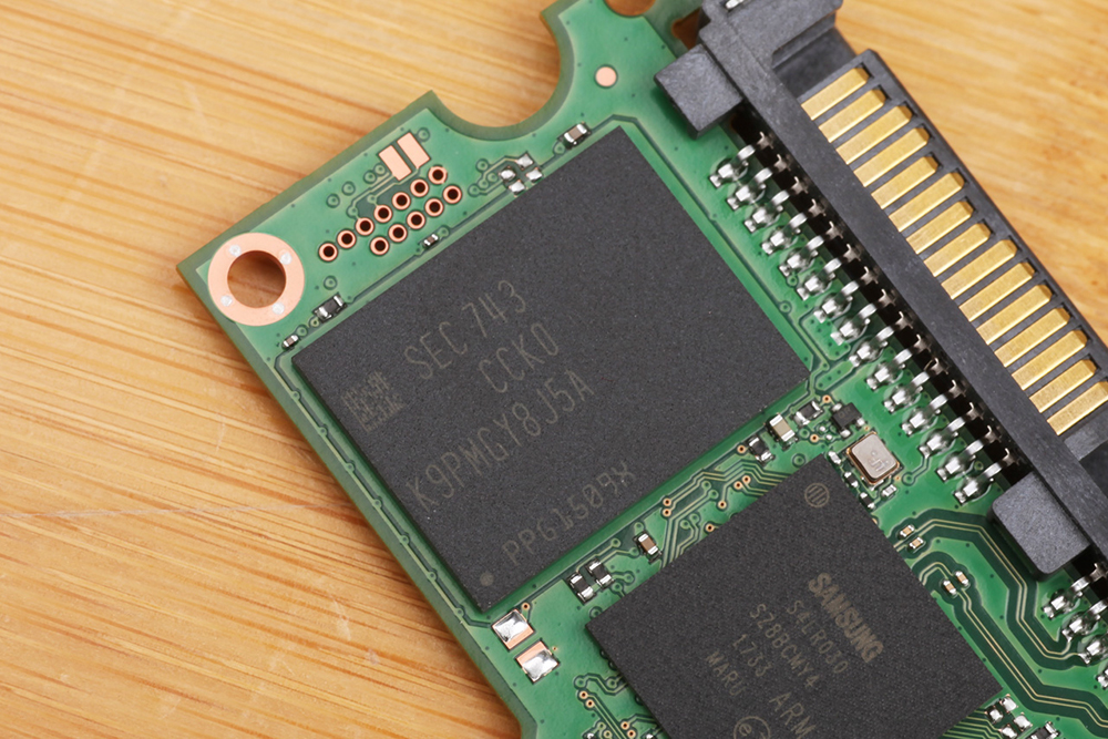
The main control unit comes from Samsung’s own MJX controller. Specific information about the MJX controller (including core number, manufacturing process, etc.) is unknown now. All we know is that it supports LPDDR4 chips.
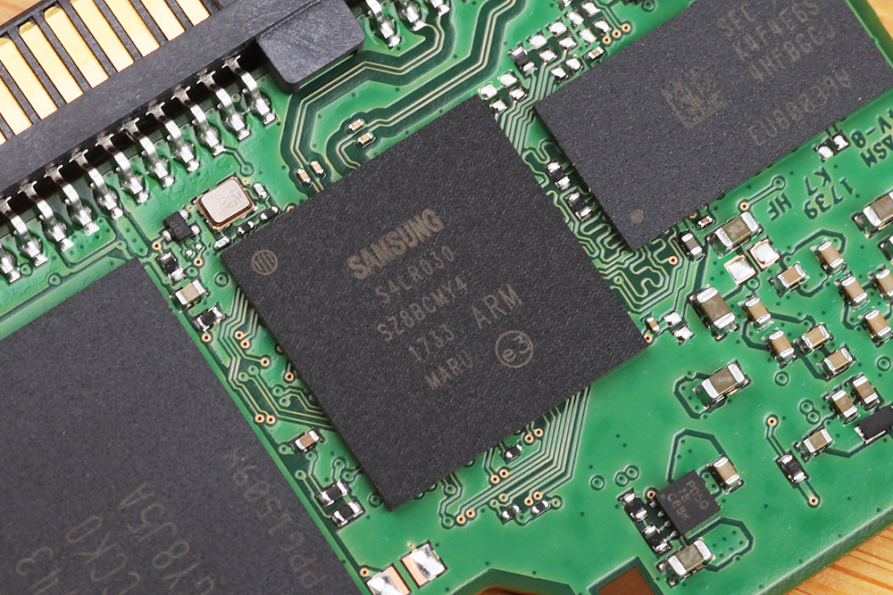
The cache chip is 512MB LPDDR4.
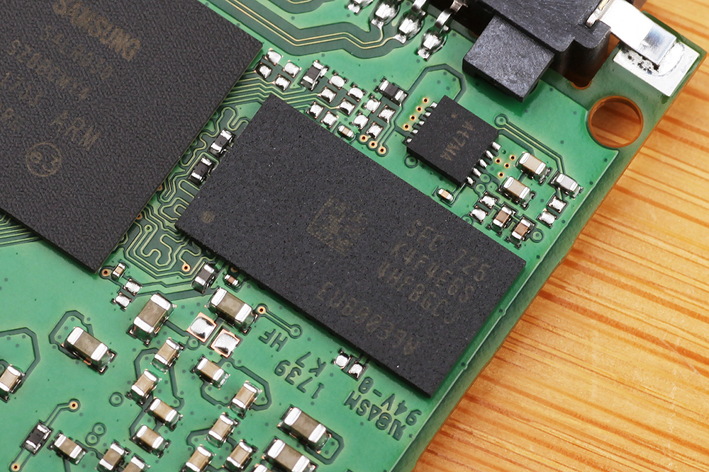
The flash is from Samsung’s 3D MLC V-NAND, which is its fourth-generation 3D NAND. The 3D MLC V-NAND has a capacity of 256 GB and a write life of 600TBW.
